


 第1年
第1年


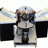
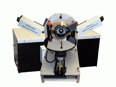
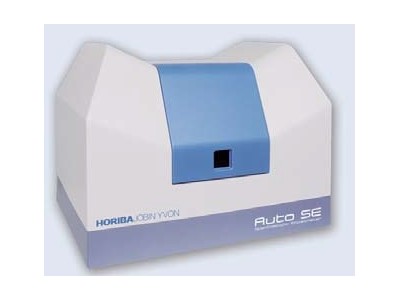
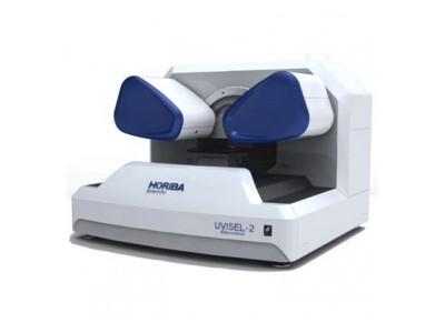
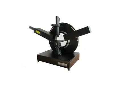
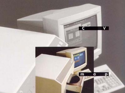
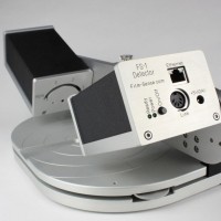
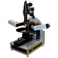
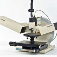
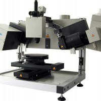
 进口四探针电阻率测试仪(4PP)/方块
- 型号:
- SE200BM/SE300BM/SE450BM/SE500BM
- 产地:
- 美国
美国赛伦科技为AST在中国地区的授权总销售服务商,赛伦科技在上海,北京分别设有办事处。
美国AST (Angstrom Sun Technologies Inc)是世界主要针对科研单位提供:spectroscopic ellipsometer (SE), spectroscopic reflectometer (SR) and Microspectrophotometer (MSP)的知名供应商。客户遍布全球主要科研大学及主要半导体厂商:
NIST
ISMI
NASA
JPL
Marshall Space Center
Air Force
MIT
Columbia University
UC Berkeley
Georgia Tech
University of Virginia
USTC,China
...
Bell Laboratories
HP
GE
Lockheed Martin
Corning
Applied Materials
First Solar
Dow Chemical
Samsung
Texas Instruments
National Semiconductor
...
美国赛伦科技上海办事处
吴惟雨/Caven Wu Cell: 13817915874
QQ:185795008 caven.wu@saratogatek.com
上海市黄浦区陆家浜路1378号万事利大厦1102室
200011
| 产品总述: | ||||
| Functions | Spectroscopic Reflectometer (SR) | Microspectrophotometer (MSP) | Spectroscopic Ellipsometer (SE) | |
| Wavelength Range | 190 to 1700 (or 2300) nm | 190 to 1700 (or 2300) nm | 190 nm to 30 µm | |
| Measurable Parameters | Film Thickness | 20Å to 250µm | 20Å to 50µm | 10Å to 10µm |
| Optical Constants | N & K | N & K | N & K | |
| R/T/A | Yes | Yes | ||
| Geometry | Yes | |||
| Digital Imaging | Yes | |||
| Main Features | Low Cost, Fast Measurement, Wide Dynamic Range | Down to 5 um Spot Size on any Patterned Structure | Complicated Layer Stack | |
| Options | Wavelength Extension, Mapping Stage, Heating/Cooling Stage | |||
| Unique Options | Large Spot Set up for In-Line Metrology Applications | Raman & Fluorescence Add-on Set-ups and optional smaller spot size | ||
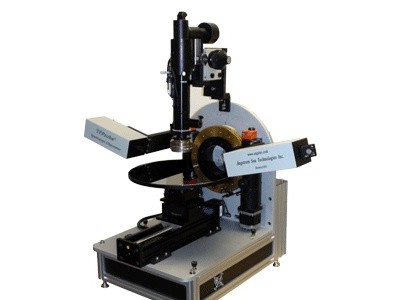
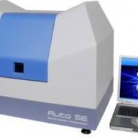
| 简介: Spectroscopic ellipsometry (SE) is a powerful technique to precisely measure thin film thickness, determine optical constants, investigate surface and interface phenomenon and many other physical, chemical and optical properties of materials. Angstrom Sun Technologies Inc designs and manufactures high quality spectroscopic ellipsometer systems with various options for different applications. Besides ellipsometer system itself, the advanced analysis software is essential to extract the desired information as above-mentioned, such as thickness, roughness, alloy concentration and dielectric constants. TFProbe™ 3.0from us offers powerful analysis functions for ellipsometry sensitivity study, photometry / ellipsometry simulation and data regression. Unique but configurable mode allows different users to access different level and suitable for both R&D and production quality control purpose. Models are specified based on wavelength ranges for different applications. The following graph shows available models for standard configurations. In addition, Model 500 simply covers a range of both Model 100 and 400. Customized products are available with wavelength range extension further down to DUV or Infrared (IR) ranges. Normally: Model 100 covers a wavelength range from DUV to NIR range up to 1100nm. Model 200 covers DUV and Visible range. Model 300 covers Visible range, starting from 370nm to 850nm Model 400 covers NIR range starting from 900nm typically Model 450 covers Vis to NIR range, starting from 370nm up to 1700nm typically Model 500 covers DUV to NIR range, up to 2500nm Model 600 covers NIR to IR range (1.7um to 17um or 1.7um to 30um) Wavelength range coverage depends on several factors such as light source, detectors, optics used in system, light delivery method (using fibers or not). Because of these factors, all tools can be customized based on specific application. For example, NIR range can be covered up to 1700nm or 2200nm or 2500nm etc. DUV range can be down to 190 nm. |
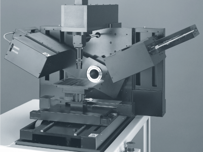
| 一。SE椭偏仪主要型号 ================================== Model SE300BM, 400-1100nm, no mapping, Model SE200BM, 250-1100nm, no mapping Model SE450BM, 400-1700nm, no mapping Model SE500BM, 190-1700nm, no mapping
6" stage mapping, adds $20K. 8" stage mapping, adds $22K. ====================================设备型号说明: Example Model: SE200BA-M300 SE: Spectroscopic Ellipsometer 200: Indicates B: Detecting Type A: Scanning monochromator with single element detector B: Array Type detector with spectrograph or interferometer A: Variable Incident Angle Type A: Automatic variable angle with precision Goniometer and computer controlled M: Manually adjustable incident angle at 5 degree interval M: Mapping Stage 300: Maximum mapping sample size |
| Options: Wavelength Extension to VUV or IR Range Stage Size Probing beam Spot size Photometry Heating/Cooling Stage Mapping stage in X-Y or Rho-Theta |
| Applications: · Semiconductor fabrication (PR, Oxide, Nitride..) · Liquid crystal display (ITO, PR, Cell gap…..) · Biological films and materials · Optical coatings, TiO2, SiO2, Ta2O5….. · Semiconductor compounds · Functional films in MEMS/MOEMS · Amorphous, nano and crystalline Si · Solar Cell Industry · Medical device fabrication |
| Background on Ellipsometry: There are many techniques for characterizing materials, each having its own advantages and disadvantages and each being uniquely able to reveal material properties that other techniques can't access. Spectroscopic ellipsometry (SE) is an optical technique that is particularly flexible in that it can be used to determine the optical and physical properties of a wide variety of thin-film materials. Its ability to do this without contact or damage to the material of interest has seen it become routinely used in R&D laboratories and within manufacturing facilities for monitoring thin film growth and deposition processes. SE relies on the determination of the polarization state of a beam of polarized light reflected from the sample under characterization. When performing SE measurements, the polarization state is determined at many discrete wavelengths over a broad wavelength range. The change in the polarization state can be traced to the physical properties of the thin film by means of a model. Characteristics such as layer thickness, surface roughness, refractive index (n) and extinction coefficient (k) of the materials can be determined with excellent precision through regression analysis. The instrument determines two ellipsometry angles Ψ and Δ, which describe the change in the polarization state of the beam upon reflection from the sample. The ratio of the amplitude of the polarization within the plane of incidence (P) to the amplitude of the polarization perpendicular to the plane of incidence (S) is represented by Ψ. The phase retardation between the two polarization vectors P and S is represented by Δ. Changes in Δ and Ψ essentially depend upon the optical constants, n and k, of the layer materials and substrate, physical thickness of the individual layers and surface roughness. A regression analysis allows the determination of these parameters. SE data for Δ and Ψ are obtained at a number of incident angles in a plane normal to the sample surface and typically at 100-200 different wavelengths for each angle. SE instruments use a white light source and individual wavelengths are selected for detection by either a motor driven monochromator, or a multi-channel detector that can detect many wavelengths simultaneously. Increasing the number of angles and wavelengths at which data are acquired improves analysis precision, especially for complicated epitaxial structures. |
| Note: 1. System configuration and Specifications subject to change without notice 2. * Film property, surface quality and layer stack dependent 3. Customized system available for special applications 4. TFProbe is registered trademark of Angstrom Sun Technologies Inc. |
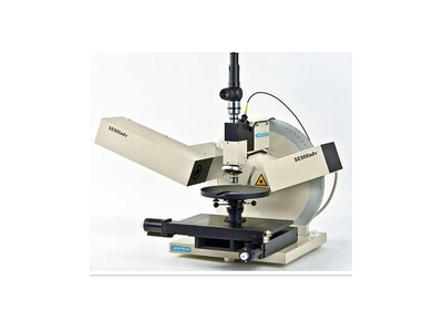
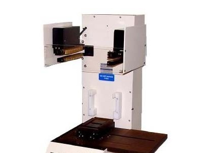
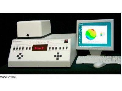
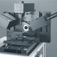
二.Microspectrophotometer(微光斑薄膜测试仪)
| MSP100 Microspectrophotometer and Film Thickness Measurement System | |
Features System Configurations Specifications Options Applications Application Examples | |
| Features:· Easy to operate with Window based software · Advanced DUV optics and rugged design for highest uptime and the best system performance · Array based detector system to ensure fast measurement · Affordable, portable and small footprint table top design · Measure film thickness and Refractive Index up to 5 layers over micron size region · Allow to acquire reflection, transmission and absorption spectra in milliseconds · Capable to be used for real time spectra, thickness, refractive index monitoring · System comes with comprehensive optical constants database and library · Advanced Software allows user to use either NK table, dispersion or composite model (EMA) for each individual film · Integrated Vision, spectrum, simulation, film thickness measurement system · Apply to many different type of substrates with different thickness up to 200mm size · Deep ultraviolet light allows to measure film thickness down to 20Å · 2D and 3D output graphics and user friendly data management interface · Advanced Imaging software for dimension measurement such as angle, distance, area, particle counting and more · Various options available to meet special applications | |
| System Configuration:· Model: MSP100RTM · Detector: CCD Array with 2048 pixels · Light Source: High power DUV-Visible · Automatic Stage: Black Anodized Aluminum Alloy with 5”x3” net travel distance and 1µm resolution, program controlled · Motorized Z focus drive and X-Y-Z joystick · Long Working Distance Objectives: 4x, 10x, 15x(DUV), 50x · Communication: USB · Measurement Type: Reflection/Transmission spectra, Film thickness/refractive index and feature dimensions · Computer: Intel Core 2 Duo Processor with 200GB Hard drive and DVD+RW Burner plus 19” LCD Monitor · Power: 110– 240 VAC /50-60Hz, 3 A · Dimension: 16’x16’x18’ (Table top setup) · Weight: 120 lbs total · Warranty: One year labor and parts | |
| Specifications: · Wavelength range: 250 to 1000 nm · Wavelength Resolution: 1nm · Spot Size: 100µm (4x), 40µm (10x), 30µm (15x), 8µm (50x) · Substrate Size: up to 20mm thick · Measurable thickness range*: 20Å to 25 µm · Measurement Time: 2 ms minimum · Accuracy*: better than 0.5% (comparing with ellipsometry results for Thermal Oxide sample by using the same optical constants) · Repeatability*: < 2 Ǻ (1 sigma from 50 thickness readings for 1500 Ǻ Thermal SiO2 on Si Wafer) | |
| Options: Top· Wavelength extension to to Further DUV or NIR range · Higher power DUV optics for smaller spot size · Customized configuration for special applications · Heating and Cooling Stage for dynamic study · Optional stage size holding samples up to 300mm · Higher wavelength range resolution down to 0.1nm · Various filters for special applications · Add-on accessories for fluorescence measurement · Add-on accessories for Raman applications · Add-on accessories for polarizing applications | |
| Applications: Top· Semiconductor fabrication (PR, Oxide, Nitride..) · Liquid crystal display (ITO, PR, Cell gap…..) · Forensics, Biological films and materials · Inks, Mineralogy, Pigments, Toners · Pharmaceuticals, Medial Devices · Optical coatings, TiO2, SiO2, Ta2O5….. · Semiconductor compounds · Functional films in MEMS/MOEMS · Amorphous, nano and crystalline Si | |
| Application Examples: Top1. Measured Transmission Spectra from Three Filters 2. Measured Film Thickness 3. Measured Reflection Spectrum over a MEMS Mirror 4. Mapped Thickness Uniformity over 4" wafer | |
| Note:1. System configuration and Specifications subject to change without notice 2. * Film property, surface quality and layer stack dependent 3. Customized system available for special applications 4. TFProbe is registered trademark of Angstrom Sun Technologies Inc. | |
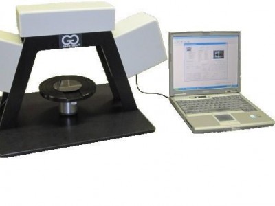
三. SR薄膜反射仪
| SRM300 Film Thickness Mapping System | |
Features System Configurations Specifications Options Applications Application Examples More Information | |
Features:Film Thickness Measurement - SRM300 Film Thickness GaugeWhen you need an accurate thin film thickness measurement our SRM300 allows you to map film thickness and refractive index up to 5 layers thick. No need to worry about complicated equipment since the SRM300 is easy to setup and operate. It uses Windows based software, so most people are already familiar with the look and feel of the operating system. This film thickness gauge can handle various types of geometry substrate up to 300mm in diameter and various types of mapping patterns such as linear, polar, square or even arbitrary coordinates. The array based detector system ensures the fastest film thickness measurement. With its advanced optics and rugged design you can always be sure to get the best system performance.· Easy to set up and operate with Window based software · Various types of geometry substrate up to 300mm in diameter · Various types of mapping pattern such as linear, polar, square or arbitrary coordinates · Advanced optics and rugged design for best system performance · Array based detector system to ensure fast measurement · Map film thickness and Refractive Index up to 5 layers · System comes with comprehensive optical constants database and library · Include commonly used recipes · Advanced TFProbe Software allows user to use either NK table, dispersion or effective media approximation (EMA) for each individual film. · Upgradeable to MSP (Microspectrophotometer) mapping system with pattern recognition, or Large Spot for mapping over patterned or featured structure (with Zonerage Model) · Apply to many different type of substrates with different thickness · 2D and 3D output graphics and user friendly data management interface with statistical results | |
| System Configuration:· Model: SRM300-300 · Detector: CCD Array with 2048 pixels · Light Source: DC regulated Tungsten-Halogen · Light Delivery: Optics · Stage1: Black Anodized Aluminum Alloy Vacuum chuck holds 200 mm wafer · Communication: USB & RS232 · Software: TFProbe 2.2M · Measurement Type: Film thickness, reflection spectrum, refractive index · Computer: Intel Core 2 Duo Processor with 200GB Hard drive and DVD+RW Burner plus 19” LCD Monitor · Power: 110– 240 VAC /50-60Hz, 3 A · Dimension: 14”(W) x 20”(D) x 14”(H) · Weight: 100 lbs · Warranty: One year labor and parts | |
| Specifications: Wavelength range: 400 to 1050 nm Spot Size: 500 µm to 5mm Sample Size: 300 mm in diameter Substrate Size: up to 50mm thick Number of Layers*: Up to 5 films Measurable thickness range*: 50 nm to 50 µm Measurement Time: 2ms - 1s /site typical Positional Repeatability: ~1 µm Accuracy*: better than 0.5% (comparing with ellipsometry results for Thermal Oxide sample by using the same optical constants) Repeatability*: < 2Ǻ (1 sigma from 50 thickness readings at center for 1500 Ǻ Thermal SiO2 on Si Wafer) | |
| Options: Top Additional Models with Wavelength Extension to DUV or NIR Range: SRM100: 250nm - 1000nm
Other Sample Size: 200mm wafer (SRM300-200) Customized size: Available Large Spot Accessories for featured structure measurement Small spot accessories for highly non uniform samples | |
| Applications: Top· Semiconductor fabrication (PR, Oxide, Nitride..) · Liquid crystal display (ITO, PR, Cell gap…..) · Biological films and materials · Optical coatings, TiO2, SiO2, Ta2O5….. · Semiconductor compounds · Functional films in MEMS/MOEMS · Amorphous, nano and crystalline Si | |
| Application Examples: Top1. 2D thicknesses plot for Nitride layer in a three layer stack (Nitride-Oxide-Nitride on Glass) 2. 2D contour plot for Nitride layer in a three layer stack (Nitride-Oxide-Nitride on Glass) | |
| Note:1. System configuration and Specifications subject to change without notice 2. * Film property, surface quality and layer stack dependent 3. Customized system available for special applications 4. TFProbe is registered trademark of Angstrom Sun Technologies Inc. | |
美国赛伦科技上海办事处
吴惟雨/Caven Wu Cell: 13817915874
QQ:185795008 caven.wu@saratogatek.com
上海市黄浦区陆家浜路1378号万事利大厦1102室
200011
注:该仪器未取得中华人民共和国医疗器械注册证,不可用于临床诊断或治疗等相关用途


 鲁公网安备37021402001368号