


 第1年
第1年


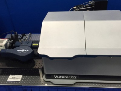
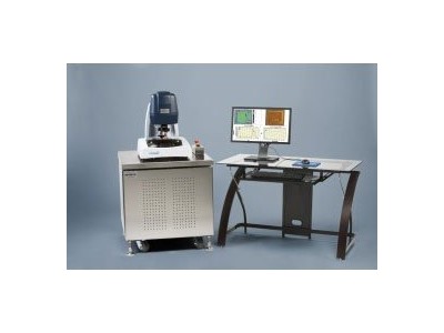
 ContourGT 非接触3D光学轮廓仪
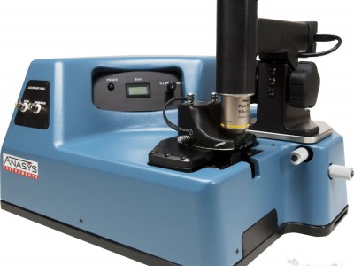
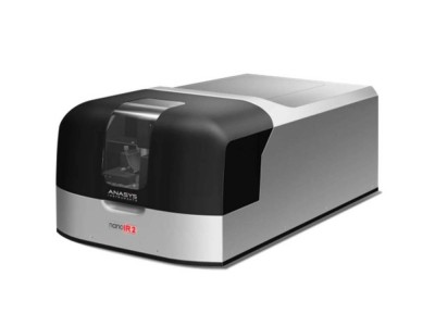
 Anasys 纳米红外&扫描近场光谱
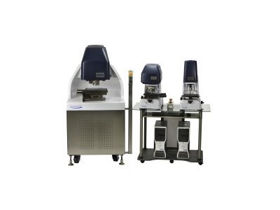
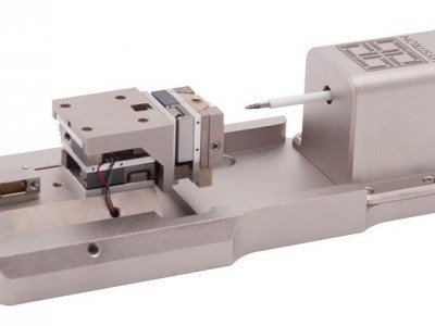
 DektakXT探针式表面轮廓仪
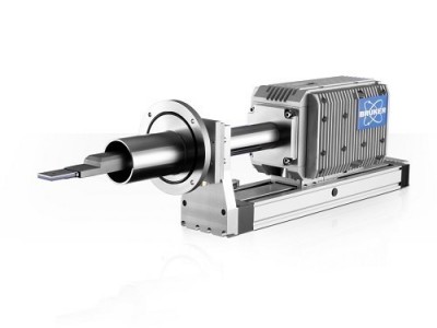
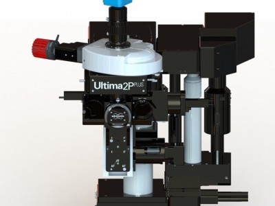 Bruker多功能双光子成像平台2pplus
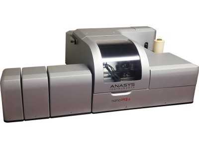
 Anasys nanoIR2-FS 快速扫描纳米红
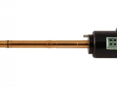
 布鲁克 PI 85L电镜专用原位纳米力学
 Bruker高品质双光子成像系统Investi
 布鲁克PI 95透射电镜专用原位纳米力
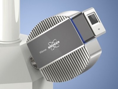
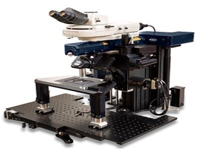
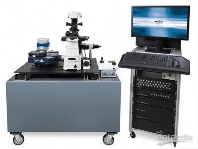 Bruker场扫描共聚焦成像系统Opterra
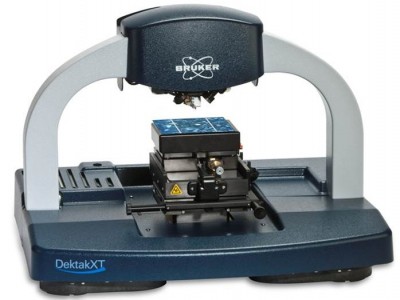
- 产地:
- 美国
- 型号:
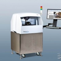
- Dektak XTL
Dektak XTL Stylus Profiler System
Bruker new Dektak XTL stylus profiler accommodates samples up to 350mm x 350mm, bringing legendary Dektak@repeatability and reproducibility to large-format wafer and panel manufacturing. The Dektak XTL features a small footprint with pneumatic passive isolation and a fully enclosed workstation with a wide, easily accessible interlocking door, making it ideal for today’s demanding production floor environments. Its dual-camera architecture enables enhanced spatial awareness, and its high level of automation maximizes manufacturing throughput. Bruker’s exclusive Vision64@ Production Interface with pattern recognition can be scaled to meet your needs and makes data collection an intuitive and repeatable process, minimizing operator-to-operator variability.
Dektak XTL Delivers
Bruker-Exclusive Dual Camera Control™
Navigate to points of interest faster by clicking in live video
Quickly orient sample to be measured by selecting twopoints in the live video (Make Horizontal)
Simplify measurement setup by point-and-click scan startand end positions in live video (Teach)
Robust Automation Setup and Operation
Accurately program fiducials and unlimited measurementsites via 300mm, automated encodedXY stage and
360-degree θ
Minimize errors utilizing Vision64 Production Interface withpattern recognition
Program custom user prompts as well as other meta datainto your recipe and store to thedatabase
Easy Analysis and Data Collection
Easily automate analysis routines using Quick Analyzer,which supports most frequently usedanalyses
Focus your analysis to report only the features needed oncomplex samples using Step Detection
Simplify data analysis by giving each measurement siteunique name and automatically log to database
Critical Resultsfor Large-Format Applications
With its unique combination of superiorperformance and ease of use, the Dektak XTLis the new QA/QC and research standardfor industrial thin film deposition monitoringin touch-panel, solar, flatpanel display, andsemiconductor industries.
Wafer Applications:
Step height for deposited thin films(metals, organics)
Step height for resists (soft film materials)
Etching rate determinations
Chemical mechanical polishing(erosion, dishing, bow)
Large Substrate Applications:
Printed circuit boards (bumps, step heights)
Window coatings
Wafer masks
Wafer chuck coatings
Polishing pads
Glass Substrate and Display Applications:
AMOLEDs
Step height measurements for LCD R&D
Film thickness measurements for touchpanels
Thin film measurements for solar coatings
Flexible Electronic Films:
Organic photodetectors
Organic films printed on films and glass
Copper traces for touch screens
Dektak XTL 探针式表面轮廓仪由布鲁克电子显微纳米分析仪器部 为您提供,如您想了解更多关于Dektak XTL 探针式表面轮廓仪报价、参数等信息 ,欢迎来电或留言咨询。


 鲁公网安备37021402001368号